The OR gate - Digital Logic gates
Gates can be combined to make combinational or sequential logic circuits. combinational circuits are a complex network of gates interconnected to evaluate a pattern of output for patterns of input.Sequential circuits use memory elements, hence output
patterns depend both on input patterns and the memory of
history of events. An example of combinational logic circuit
is a seven segment display decoder CD4511 and and example for
a sequential logic circuit is CD4029 up-down counter.
Usage of Schmitt trigger NAND Gate
OR Gate Simulation
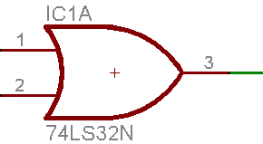
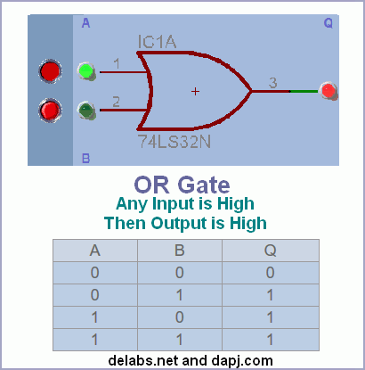
This gate ORs the two inputs A and B, The Output is high if either A OR B is high. There may be a OR gate with many inputs, if one or more inputs are high then the output will be high. AND and OR gates can be wired with Diode logic.
This page requires images and javascript to be enabled
to try out the demo of the gates below.
| A | Q | |||
 |
||||
| B | |
Toggle the red buttons above to apply a 'high' or 'low' to inputs A and B and watch the output Q.
Truth table
| A | B | Q |
| 0 |
0 | 0 |
| 0 | 1 | 1 |
| 1 | 0 | 1 |
| 1 |
1 | 1 |
Interactive Digital Logic Gates Tutor Widget
Interactive Tutor for Learning Digital Logic, Like NOT, AND, OR and XOR.
OR gate with two 555
These Gadgets helps beginners learn some digital circuit concepts. The Digital Logic is Studied by operating Switches and observing LEDs on a Virtual Breadboard. Lead Free
Screenshot

...
...
...
...
...
delabs Technologies
30th Aug 2020
...
The documents, software, tools and links are provided to enhance the ability of an electronics student, hobbyist or professional by sharing information. The information, links etc. should be used by the website visitor, at his or her own risk and responsibility. There may be concept, design and link errors in the pages.
Creative Work, ideas and documents of delabs can be used for Product Design and Development by R&D Engineers, Hobbyists, Students and even firms for creating useful products. These cannot be used for reprint, replication or publishing online or offline.

