Single Digit Voltmeter with LM311
I wanted to design a logic probe as a tutorial, but there were many good ones in the web so i have tried to design a single digit voltmeter. This circuit is a design, i am unable to test it now, later if i test it and find mistakes i will update this page. You can help me by pointing out the errors.
Data Interface – Printer Port, Virtual Instrumentation.

First bear it in mind that it is a single digit voltmeter which is 0-9 counts only on the positive side, that is it can measure +0 to +9V DC +/- 1V error. That may not be practical for the cost of the components above. It may be used as a toy logic probe. The reason for the circuit is not for usage, but to give design ideas. The methodology used is Gut Feel – Thumb Rule method.
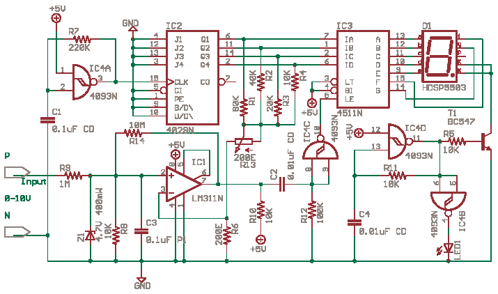
First i explain the simple part, D1 a seven segment common cathode LED display is chosen as CD4511 is a sourcing driver. 4511 can be latched so it has been used here, it decodes binary 4 bit decade info to seven segment output. The four bits are derived from CD4029 up-down clock pulse counter. LM311 is a analog comparator with single supply capability which is the A-D interface.
To avoid resistors for each of the LEDs the LEDs are turned ON-OFF at 10KHz 50% duty cycle. The Nand Schmitt Trigger CD4093 is used as in IC4D as a 10KHz Clock which drives T1 transistor with a resistor R5. On turn on IC4D one input is high which is pin 12 pulled up to +5 and another Pin 13 is Low as C4 is in discharged condition in NAND gate both inputs high, gives a low output, the other combinations the output is high. So the output goes high, this starts charging the cap C4 which soon makes both inputs high, which in turn makes output low starting the discharge of C4. This is now evidently a endless loop, hence it is a oscillator. R*C = T …. 0.01uF * 10K = 100uS or 10KHz as F=1/T approx or better still multiply by 1.1 ?. I am not good at formulae but i manage with a calculator.
The supply and ground pins of CMOS chips have not been shown, see datasheet or earlier circuits.
IC4A is also a oscillator but slower which is good enough, it is slow so that a measurement can be made nearly every second. The IC4A slow clock is read by 4029 which produces a count-down binary nibble at Q1….Q4, This is converted to crude analog with R1…R4. The voltage generated is compared with the voltage you are measuring by LM311 which generates a Latch pulse to 4511 to freeze the reading where both voltages match.
Method of Operation :
IC2 is a Counter in Decade-Down mode and IC3 is a BCD to Seven Segment Decoder which Drives the Display D1. The Circuit is wired in such a way as to keep counting the Pulses from the Clock IC4A. The IC4A which is wired as Schmitt Nand Oscillator Clocks the Counter. Now to understand how this Counter and display works see this Interactive Tutorial Simple Digital Counter. For every pulse at Pin-15 of 4029 the Counter Counts down from 9-8-7-6…. and so on. But the Display is Latched by IC4C, So the Display is static even when counter is running. So while testing counter you can remove IC4C and keep LE Pin-5 of 4511 low to ground. For testing this Circuit you can use the manual clock with a pushbutton (single step) or a slow clock rate 1 Hz as in the Tutorial Simple Digital Counter.
The Transistor T1 and Oscillator IC4D is to chop the power to display at a fast rate, this avoids the adding of seven resistors. This is not required, but it saves power and reduces parts count. IC4B is is like a ON indicator, it is a spare gate.
The BCD value at output of 4029 Q1-Q4, four bits, a nibble, is converted to an analog mV value across R6. The resistors R1-R4 which are connected to Q1-Q4 have weighted resistor values for the BCD 1-2-4-8. By ohms law you can understand that the analog value across R6 is approximately proportional to the BCD value. This circuit is just a single digit A-D converter, not even as good as 4 bit converter. Which means approximate value of analog at R6 will do.
Now lastly LM311 is a Comparator, it compares the Analog BCD reference at Pin-3 and the Attenuated Input signal at Pin-2. Output Pin-7 goes high when Pin-3 voltage becomes less than Pin-2. This is made to a narrow latch pulse by C2-R12-IC4C. The latch pulse freezes the BCD data to display till the next latch pulse. R8-R9 attenuate the 0-9 V DC input to a 1/100 value. The zener Diode Z1 is for protection.
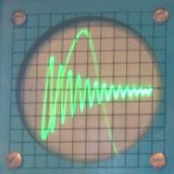
I guess the LM311 circuit should work off a single supply, but a dual supply may be required as voltage levels may be near zero. You must be able to see a staircase waveform or ramp across R6. Narrow Latch pulses at Pin-5 4511 on every ramp cycle.