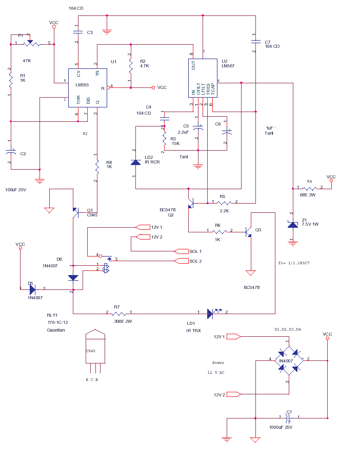
Optical obstacle switch - del50006
This is a simple toy that has many applications. Any object that breaks a light beam will trigger a relay to on condition for a period of time.Description - The 555 monostable has a 1 second period, If pin 2 gets low trigger pulses of a frequency more than 1 Hz, the output pin 3 will remain high, if the trigger pulses came in 10 second delays then output will go on and off, so also the relay and the electrical load on relay contacts. Like an integrator, it will not operate relay very fast. Even in a fridge stabilizer they put something like this else the compressor motor is damaged on frequent black-brown outs.
Optical Retro-Reflective Proximity Switch
Now for the LM567 part, The clock at pin 5 flashes the IR Transmitter LED LD1 at a frequency set by C7-R5. The IR Photo Sensitive Diode or Transistor LD2 conducts when light is got from the IR LED. As the lights is in pulses, so also the impedance of LD2 goes low and high at same frequency.
This develops an AC waveform across R3 over a DC representing Ambient light. If direct sunlight falls on this arrangement, the Photo-diode saturates, then this circuit or any other circuit won't work. But when ample protection from ambient light is made, some pulses good enough for LM567 tone detection, 100mV rms, is obtained and it operates the relay via a LM555.

Component Layout Hand-Made Artwork Positive Film Solder Mask
Right Click Image, Save to Disk, Print to Scale.
Build it Yourself.
The Artwork was made by a traditional PCB Artist with Artwork tape, pads, Rotring Pen, and Knife. This is scan of Hand-Made Artwork. Then we go to a Offset printing, photo processing studio, he will make a Positive and Negative of artwork with photography. This is what you will need to make a PCB. Positive Film and Solder Mask.Optical switch with photo sensors
The Artwork and Film are 1:1 or 1x, 300dpi scan. The Solder Mask is shrunk to 1/2, it may not be usable, i have to still build some graphics expertise and using the scanner. The component layout is an assembly instruction. I have no idea how you will make PCBs out of this, try postscript printing or ask a DTP professional.
But if you manage to get a scaled print, and you know screen printing or even have a photo resist fluid. you can make prototypes at home. I used to do it in my younger days.
...
...
...
...
...
delabs Technologies
20th Mar 2020
...
Disclaimer and Terms of usage
The documents, software, tools and links are provided to enhance the ability of an electronics student, hobbyist or professional by sharing information. The information, links etc. should be used by the website visitor, at his or her own risk and responsibility. There may be concept, design and link errors in the pages.
Creative Work, ideas and documents of delabs can be used for Product Design and Development by R&D Engineers, Hobbyists, Students and even firms for creating useful products. These cannot be used for reprint, replication or publishing online or offline.

